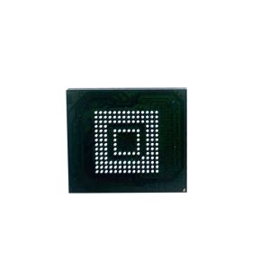
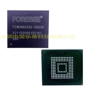
FEMDNN008G-08A39 BGA-153 8G EMMC Flash Memory Chip
Features
- eMMC5.1 specification compatibility(Backward compatible to
eMMC4.41/4.5/5.0)
- Bus mode
- Data bus width: 1 bit (default), 4 bits, 8 bits
- Data transfer rate: up to 400MB/s (HS400)
- MMC I/F Clock frequency : 0~200MHz
- Operating voltage range
- Vcc(NAND) : 2.7 - 3.6V
- Vccq(Controller) : 1.7 - 1.95V / 2.7 - 3.6V
- Temperature
- Operation (-25℃ ~ +85℃)
- Storage without operation (-40℃ ~ +85℃)
- Sudden-Power-Loss safeguard
- Hardware ECC engine
- Unique firmware backup mechanism
- Global-wear-leveling
- Supported features.
- HS400, HS200
- Partitioning, RPMB
- Boot feature, boot partition
- HW Reset/SW Reset
- Discard, Trim, Erase, Sanitize
- Background operations, HPI
- Enhanced reliable write
- S.M.A.R.T. Health Report
- FFU
- Sleep / awake
- Others
- Compliance with the RoHS Directive
Functional Description
FORESEE eMMC with powerful L2P (Logical to Physical) NAND Flash
management algorithm provides unique functions:
- Host independence from details of operating NAND flash
- Internal ECC to correct defect in NAND flash
- Sudden-Power-Loss safeguard
Sudden-Power-Loss safeguard
To prevent from data loss, a mechanism named Sudden-Power-Loss
safeguard is added in the eMMC. In the case of sudden
power-failure, the eMMC would work properly after power cycling.
Global-wear-leveling
To achieve the best stability and device endurance, this eMMC
equips the Global Wear Leveling algorithm. It ensures that not only
normal area, but also the frequently accessed area, such as FAT,
would be programmed and erased evenly.
IDA(Initial Data Acceleration)
The eMMC prevents the pre-burned data from data-loss with IDA, in
case of our customer had pre-burned data to eMMC, before the eMMC
being SMT.
Cache
The eMMC enhanced the data written performance with Cache, with
which our customer would get more endurance and reliability.
Partition Management
The embedded device offers also the possibility of configuring by
the host additional split local memory partitions with independent
addressable space starting from logical address 0x00000000 for
different usage models. Default size of each Boot Area Partition is
4096 KB and can be changed by Vendor Command as multiple of 128KB.
Boot area partition size is calculated as ( 128KB * BOOT_SIZE_MULTI
) The size of Boot Area Partition 1 and 2 cannot be set
independently and is set as same value Boot area partition which is
enhanced partition. Therefore memory block area scan is classified
as follows:
- Factory configuration supplies boot partitions.
- The RPMB partition is 4MB.
- The host is free to configure one segment in the User Data Area to
be implemented as enhanced storage media, and to specify its
starting location and size in terms of Write Protect Groups. The
attributes of this Enhanced User Data Area can be programmed only
once during the device life-cycle (one-time programmable).
- Up to four General Purpose Area Partitions can be configured to
store user data or sensitive data, or for other host usage models.
The size of these partitions is a multiple of the write protect
group. Size and attributes can be programmed once in device
life-cycle (one-time programmable). Each of the General Purpose
Area Partitions can be implemented with enhanced technological
features.
Pin Descriptions
- CLOCK(CLK)
- Each cycle of the clock directs a transfer on the command line and
on the datalines.
- COMMAND(CMD)
- This signal is a bidirectional command channel used for device
initialization and command transfer. The CMD Signal has 2 operation
modes: open drain, for initialization, and push-pull, for command
transfer. Commands are sent from the host to the device, and
responses are sent from the device to the host.
- DATA(DAT0-DAT7)
- These are bidirectional data signal. The DAT signals operate in
push-pull mode. By default, after power-up or RESET, only DAT0 is
used for data transfer. The controller can configure a wider data
bus for data transfer wither using DAT[3:0](4bit mode)or
DAT[7:0](8bit mode). Includes internal pull-up resistors for data
lines DAT[7:1]. Immediately after entering the 4-bit mode, the
device disconnects the internal pull-up resistors on the DAT1 and
DAT2 lines.(The DAT3 line internal pull-up is left connected.) Upon
entering the 8bit mode, the device disconnects the internal pull-up
on the DAT1, DAT2, and DAT[7:4]lines.
- Data Strobe(DS)
- Newly assigned pin for HS400 mode. Data Strobe is generated from
e.MMC to host. In HS400 mode, read data and CRC response are
synchronized with Data Strobe.
- RESET(RSTN)
- Hardware Reset Input
- Vccq
- Vccq is the power supply line for host interface, have two power
mode: High power mode:2.7V~3.6V; Lower power mode:1.7V~1.95V
- Vcc
- Vcc is the power supply line for internal flash memory, its power
voltage range is:2.7V~3.6V
- VDDi
- VDDi is internal power node, not the power supply. Connect 1uF
capacitor VDDi to ground
- Vss,Vssq
- Ground lines
Packaging & Shipping
Standard export packaging available. Customers can choose from
cartons, wooden cases, and wooden pallets according to their
requirements.
Frequently Asked Questions
How to obtain the price?
We typically provide quotations within 24 hours of receiving your
inquiry (excluding weekends and holidays). For urgent pricing
requests, please contact us directly.
What is your delivery time?
Small batches typically ship within 7-15 days, while large batch
orders may require approximately 30 days depending on order
quantity and season.
What are your payment terms?
Factory pricing with 30% deposit and 70% balance payment via T/T
before shipment.
What are the shipping options?
Available shipping methods include sea freight, air freight, and
express delivery (EMS, UPS, DHL, TNT, FEDEX). Please confirm your
preferred method before ordering.


