Sign In | Join Free | My himfr.com
Home > DRAM Memory Chip >

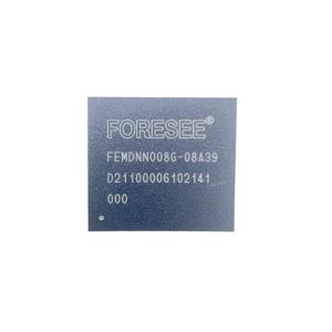
FEMDRW064G88A19 BGA153 EMMC Memory Chip

    Buy cheap FEMDRW064G88A19 BGA153 EMMC Memory Chip from wholesalers
     
    Buy cheap FEMDRW064G88A19 BGA153 EMMC Memory Chip from wholesalers
    • Buy cheap FEMDRW064G88A19 BGA153 EMMC Memory Chip from wholesalers
    • Buy cheap FEMDRW064G88A19 BGA153 EMMC Memory Chip from wholesalers
    • Buy cheap FEMDRW064G88A19 BGA153 EMMC Memory Chip from wholesalers

    FEMDRW064G88A19 BGA153 EMMC Memory Chip

    Ask Lasest Price
    Brand Name : FORESEE
    Model Number : FEMDRW064G-88A19
    Certification : ROHS
    Price : consult
    Payment Terms : T/T,Western Union
    Supply Ability : 100000
    Delivery Time : 5-8day
    • Product Details
    • Company Profile

    FEMDRW064G88A19 BGA153 EMMC Memory Chip

    FEMDRW064G88A19 BGA153 EMMC Memory Chip
    KEY FEATURES
    • eMMC5.1 specification compatibility- Backward compatible to eMMC4.41/4.5/5.0
    • Bus mode
      • Data bus width: 1 bit (default), 4 bits, 8 bits
      • Data transfer rate: up to 400MB/s (HS400)
      • MMC I/F Clock frequency: 0~200MHz
    • Operating voltage range
      • VCC(NAND): 2.7 ~ 3.6V
      • VCCQ(Controller): 1.7 ~ 1.95V / 2.7 ~ 3.6V
    • Temperature
      • Operation: -40℃ ~ +85℃
      • Storage without operation: -40℃ ~ +85℃
    • Sudden-Power-Loss safeguard
    • Hardware ECC engine
    • Unique firmware backup mechanism
    • Global-wear-leveling
    • Supported features.
      • HS400, HS200
      • Partitioning, RPMB
      • Boot feature, boot partition
      • HW Reset/SW Reset
      • Discard, Trim, Erase, Sanitize
      • Background operations, HPI
      • Enhanced reliable write
      • S.M.A.R.T. Health Report
      • FFU
      • Sleep / awake
    • Others
      • Compliance with the RoHS Directive
    Functional Description

    FORESEE eMMC with powerful L2P (Logical to Physical) NAND Flash management algorithm provides unique functions:

    • Host independence from details of operating NAND flash
      The eMMC Controller already includes Flash management technologies such as data storage and retrieval, defect handling and diagnostics, and power management. Host can be free from considering about NAND Flash data operating.
    • Internal ECC to correct defect in NAND flash
      The hardware error correction code (ECC) function, which can prevent data corruption data corruption is included in the eMMC controller.
    • Sudden-Power-Loss Safeguard
      To prevent from data loss, a mechanism named Sudden-Power-Loss Safeguard is added in the eMMC. In the case of sudden power-failure, the eMMC would work properly after power cycling.
    • Global-wear-leveling
      To achieve the best stability and device endurance, this eMMC equips the Global Wear Leveling algorithm. It ensures that not only normal area, but also the frequently accessed area, such as FAT, would be programmed and erased evenly.
    • IDA (Initial Data Acceleration)
      The eMMC prevents the pre-burned data from data-loss with IDA, in case of our customer had pre-burned data to eMMC, before the eMMC being SMT.
    • Cache
      The eMMC enhanced the data written performance with Cache, with which our customer would get more endurance and reliability
    Partition Management

    The embedded device offers also the possibility of configuring by the host additional split local memory partitions with independent addressable space starting from logical address 0x00000000 for different usage models. Default size of each Boot Area Partition is 4096 KB and can be changed by Vendor Command as multiple of 128KB. Boot area partition size is calculated as (128KB * BOOT_SIZE_MULTI) The size of Boot Area Partition 1 and 2 cannot be set independently and is set as same value Boot area partition which is enhanced partition. Therefore, memory block area scan is classified as follows:

    • Factory configuration supplies boot partitions.
    • The RPMB partition is 4MB.
    • The host is free to configure one segment in the User Data Area to be implemented as enhanced storage media, and to specify its starting location and size in terms of Write Protect Groups. The attributes of this Enhanced User Data Area can be programmed only once during the device life-cycle (one-time programmable).
    • Up to four General Purpose Area Partitions can be configured to store user data or sensitive data, or for other host usage models. The size of these partitions is a multiple of the write protect group. Size and attributes can be programmed once in device life-cycle (one-time programmable). Each of the General-Purpose Area Partitions can be implemented with enhanced technological features.
    Pinout Description
    Pin No.Pin NameDescription
    K5RSTNHardware Reset Input
    C6VCCQVCCQ is the power supply line for host interface, have two power mode: High power mode:2.7V~3.6V;Lower power mode:1.7V~1.95V.
    M4VCCQVCCQ is the power supply line for host interface, have two power mode: High power mode:2.7V~3.6V;Lower power mode:1.7V~1.95V.
    N4VCCQVCCQ is the power supply line for host interface, have two power mode: High power mode:2.7V~3.6V;Lower power mode:1.7V~1.95V.
    P3VCCQVCCQ is the power supply line for host interface, have two power mode: High power mode:2.7V~3.6V;Lower power mode:1.7V~1.95V.
    P5VCCQVCCQ is the power supply line for host interface, have two power mode: High power mode:2.7V~3.6V;Lower power mode:1.7V~1.95V.
    E6VCCVCC is the power supply line for internal flash memory, its power voltage range is:2.7V~3.6V.
    F5VCCVCC is the power supply line for internal flash memory, its power voltage range is:2.7V~3.6V.
    J10VCCVCC is the power supply line for internal flash memory, its power voltage range is:2.7V~3.6V.
    K9VCCVCC is the power supply line for internal flash memory, its power voltage range is:2.7V~3.6V.
    C2VDDiVDDi is internal power node, not the power supply. Connect 1uF capacitor VDDi to ground.
    M5CMDThis signal is a bidirectional command channel used for device initialization and command transfer.Commands are sent from the host to the device, and responses are sent from the device to the host.The CMD Signal has 2 operation modes: open drain for initialization, and push-pull for command transfer.
    H5DSData Strobe signal. Newly assigned pin for HS400 mode. Data Strobe is generated from eMMC to host.In HS400 mode, read data and CRC response are synchronized with Data Strobe.
    M6CLKEach cycle of this signal directs a one-bit transfer on the command and either a one-bit (1x) or a twobits transfer (2x) on all the data lines.
    J5VSSGround connections
    A6VSSGround connections
    C4VSSGround connections
    E7VSSGround connections
    G5VSSGround connections
    H10VSSGround connections
    K8VSSGround connections
    N2VSSGround connections
    N5VSSGround connections
    P4VSSGround connections
    P6VSSGround connections
    Packaging & Shipping

    Standard export packaging available. Customers can choose from cartons, wooden cases, and wooden pallets according to their requirements.

    Frequently Asked Questions

    How to obtain the price?

    We typically provide quotations within 24 hours of receiving your inquiry (excluding weekends and holidays). For urgent pricing requests, please contact us directly.

    What is your delivery time?

    Small batches typically ship within 7-15 days, while large batch orders may require approximately 30 days depending on order quantity and season.

    What are your payment terms?

    Factory pricing with 30% deposit and 70% balance payment via T/T before shipment.

    What are the shipping options?

    Available shipping methods include sea freight, air freight, and express delivery (EMS, UPS, DHL, TNT, FEDEX). Please confirm your preferred method before ordering.

    Quality FEMDRW064G88A19 BGA153 EMMC Memory Chip for sale
    Inquiry Cart 0
    Send your message to this supplier
     
    *From:
    *To: Shenzhen Filetti Technology Co., LTD
    *Subject:
    *Message:
    Characters Remaining: (0/3000)